About Us
Protection against zero-day vulnerabilities in just 2 hours
.jpg)

Protection against zero-day vulnerabilities in just 2 hours
.jpg)
R.Q.S Trade Service CO., Limited is the professional SUPPLIER of AI(Auto Insertion )/SMT (Surface-Mount Technology) spare parts, Board Handling System equipments and SMT Peripheral equipments and consumables which located in Shenzhen China , integrating production, manufacturing and trade.
.jpg)
“Reliability ,Quality , Service” is our FOUNDATION !
“The parts that can’t be bought ask help of R.Q.S. Trustworthy not only products but also us !
“Solving the problem of electronic product production” is our MISSION.
“Quality First ,Customer satisfaction , Breakthrough, Unity and Win-Win” is our core VALUE.
“To be a worldwide One Stop AI/SMT PROVIDER . The supplier for AI/THT/SMT (Auto Insertion/Through Hole Technology / Surface mount Technology) Machines Spare Parts ,the Board Handling System equipments, Peripheral Equipments and Consumables .” is our GOLD .
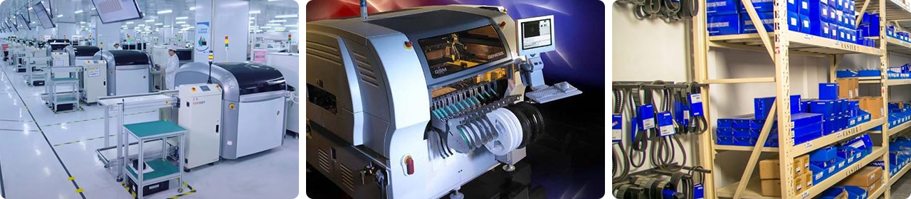
WE Focus on Supplying One-Stop Spare Parts for AI/SMT Machines , Professionally provide High quality and Lowest Ex-factory Price for Peripheral Equipments and Workshop Consumables !
1) For SMT Pick & Place Equipment and Auto Insertion Machine brands : *AI machine brand parts : Universal (UIC), Panasonic ,TDK ,Sciencgo *SMT machine brand parts : Universal, Panasonic , FUJI , Samsung, JUKI, YAMAHA, DEK, ASM, SONY, Philips, SANYO, HITACHI, etc. For example: Vacuum Nozzles, Feeder and its Accessories, Filters, Ball screw, Cutter Blades, Glue Dispenser Nozzles, Vacuum Pumps and Accessories,Springs, Lamps, Belts,Motor,Driver and more!
2) PCB Board Handling System : Conveyor ,Auto Loader ,Auto Unloader, Screen Printer ,Parallel transfer machine, Micro board machine, NG/OK PCB board collection machine, Etc. Meanwhile ,R.Q.S Support Customizing the special board handling system for customers requirements !
3) For Workshop Consumables&Peripheral Equipments: SMT ESD Magazine Rack ,Feeder Carts ,Stencil Wiper , Splice Tape for AI &SMT , KIC Profiler , Thermocouple wire and Plug , Splice tape Plier ,Components counters, Solder Paste mixer, PCB Cleaner etc.
4) R.Q.S Provide full training for AI SMT processing, machine installation, troubleshooting, maintenance, and upgrade .
We always be here for any of your requirement. Email: info@aismthelp.com